Contact Person: Frivy Flex
E-mail: Frivy.Flex@iacslight.com
skype: fobfrivy@gmail.com
Add: Pengjiang Distribution, Jiangmen City, Guangdon Province, China


The Technology Trend of LED Driver for LED Display Applications: AC Responses
Foreword
AC responses of LED drivers are critical truly ignored in LED display applications. AC responses affect the major performance of LED display panels, like grayscales, linearity, EMI, and reliability. To find out trade-off within these requirements, LED drivers provides balance. This article further explain the need for the AC responses of LED drivers and PCB design strategies to help engineers to create LED panels with higher grayscale images.
Minimum OE pulse width vs. Linearity
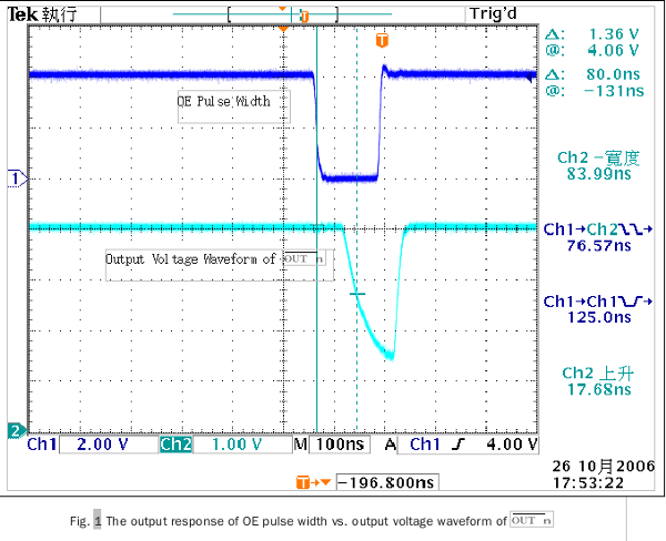
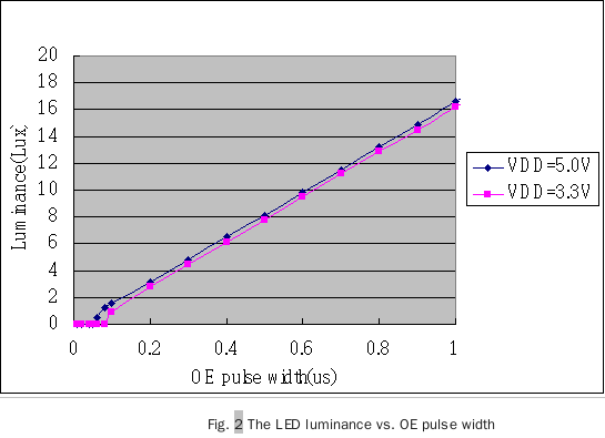
LED panel manufacturers are asking more on the grayscale improvement to enhance hue of image on LED panels which satisfy audiences more. Over 1024 grayscales of every color has become a common requirement for full color LED panels. On the same clock frequency, short OE pulse width and response time (tr / tf) may help get more jobs done grayscales. Yet, design for short OE pulse width sacrifices the linearity, this means the proportion relating to the input data and output brightness. For example, the output voltage waveform of in Fig.1 is shorter as opposed to OE pulse width, and the linearity outcome is shown in Fig.2. Obviously, the linearity of LED luminance is not really proportional on the setting of OE pulse width specially when OE pulse width is lower than .1us. Therefore, the linearity is not good for this issue.
There are several definitions of minimum OE pulse width on the market. Some vendors define it as being the shortest OE pulse width that output voltage of can respond to, however this definition is simply meaningful under good linearity condition.
Overshoot Elimination
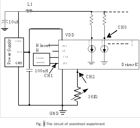
The voltage overshoot on the output channels usually damages the LED driver, when an LED driver is deterred. This influences the toughness for LED panels. The voltage overshoot results from the parasitic inductance between VLED and OUTn (output ports). Fig. 3 and Fig. 4 explain the experiment connection between the voltage overshoot. Inside the experiment, inductors are put into the circuit to simulate the parasitic inductors from the PCB traces. The waveform on node CH1~CH3 in Fig.3 are provided in Fig. 4 respectively. The voltage around the output node (CH3) will reach 26.6V, that is much higher as opposed to breakdown voltage (17V) of your LED driver.
The overshoot voltage may be calculated from the formula below:
V = L x di / dt
where V could be the induced surge voltage
L will be the parasitic inductance
di / dt may be the current variation during switching.
You'll find three ways to remove the voltage overshoot. First approach would be to decrease the parasitic inductances. As the VLED overshoot may also accumulate on the VOUT surge, the traces of utility lines every individual output channel should be as little as possible and the distributed capacitors between VLED and GND should be placed uniformly for the PCB to lessen the overshoot on VLED and VOUT.
The second approach would be to switch the driving devices slowly. LED drivers with short response time (tr / tf) are not suggested as it may cause higher voltage surge. Choosing an LED driver with moderate response time (tr / tf) for various applications is plenty.
The next way is to disperse the switching noise. LED panel manufacturers may choose LED drivers with staggered output delay of each and every channel to stop all output channels to exchange at the same time. By the staggered output delay between channels, the overshoot could be suppressed.
Conclusion
Carefully choosing LED drivers and designing with higher PCB routing as instructed above help LED panel manufacturers help the grayscales and robustness of LED panels. The most recent LED drivers in the marketplace, including MBI5025 and MBI5039, provide balance to help LED panel manufacturers easily achieve better image quality on LED panels with higher system reliability.
